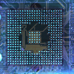
Unlike surface mount components with leads around the perimeter (i.e. QFP, SOIC), Ball Grid Array (BGA) packages contain a matrix of solder spheres on the bottom side. From a design standpoint, one of the benefits that a BGA offers versus a part with leads is having a greater number of connections over the same amount of die size.
The disadvantage, however, is that those connections are now hidden making rework a more complicated process requiring specialized equipment. This article details the steps of reworking a BGA device on a circuit board using an AT-GDP Rework Station. A Pb-Free profile has been applied during soldering and desoldering processes.
Device and PCB
There are several sources for how a reflow profile graph should look like. The most common are solder paste and component BGA measures 31mm x 31mm (1.22” x 1.22”) and contains 421 spheres (Figure 1). Solder spheres measure 0.6mm in diameter with a pitch of 1.0mm. Printed Circuit Board (PCB) measures 229mm x 305mm x 1.52mm thick (9“ x 12” x 0.060”).

Figure 1: BGA on a PCB
Desoldering
After securing the circuit board on the machine’s stage, an operator installs a vacuum pick-up tip and nozzle suitable for the BGA device. Implementing machine optics, the nozzle is aligned over the component. A pre-established profile is selected from the software’ library and the Start icon is selected. At this point the process is hands-off. The rework station automatically drives the nozzle down to a board and covers the BGA. The machine then activates the vacuum pick-up tip so as to remove the component once reflow is achieved and the heating cycle is initiated. Figure 2 shows a nozzle covering the device during reflow.
Heating is precisely controlled by the software (Figure 3). It mimics an original reflow profile with heat applied from both the top and bottom sides of a circuit board. The Source of bottom heating is Quartz IR while the top side is forced air or nitrogen convection. Upon completion of reflow, the machine lifts a BGA off a board and moves the nozzle up along the Z axis to its starting point.

Figure 2: Nozzle covering BGA during reflow
 Figure 3: Screenshot of a reflow profile
Residual solder will remain on the circuit board after removing a component. It will be irregular in shape and in some cases may look like a Hershey’s kisses candy due to the surface tension of molten solder as the part comes up. As a result of its uneven shape and volume, solder must be removed prior to soldering a new component (Figure 4). This may be accomplished by using a vacuum de-soldering tool or more commonly by wicking solder with a copper braid and soldering iron.

Figure 4: Board pads after cleaning off excess solder
Alignment, Placement, and Soldering
Once PCB pads have been cleaned to remove residual solder, the component may be aligned, placed, and soldered to the circuit board. After the BGA has been picked up by the rework station, the next step involves transferring tacky flux or solder paste to spheres of a device.
Both may be applied by dipping the component in a universal transfer plate. Implementing tacky rework flux, however, is more common. As displayed in Figure 5, the BGA is dipped into a Flux Transfer Plate (Part: FTP-ATGDP) that contains a pool of tacky flux 300µm deep. Now the tip of each of the 421 solder spheres contains a small amount of flux that is necessary for proper wetting and joint formation.

Figure 5: BGA dipped in flux
The component is now ready to be optically aligned over the matching pads on a circuit board. As the Split Vision Optics arm is moved into position (Figure 8). It enables viewing solder spheres of a BGA and pads of a board simultaneously on the same screen. Magnification and LED lighting intensity may be adjusted to create optimum solder sphere size and contrast between the two images.
Figure 6 shows a camera view screenshot where solder spheres and pads are misaligned. By adjusting the X-Y micrometers of a vacuum lockable board holder and theta rotation adjustment, BGA’s spheres were aligned over the board’s pads (Figure 7). The component is now ready to be placed and soldered.

Figure 6: Solder spheres and pads misaligned

Figure 7: Solder spheres and pads aligned

Figure 8: Split Vision Optics arm in position
Upon moving the optics arm to its original position, the device may now be placed on a board and solder reflowed. As in the removal process, the same pre-established profile is selected from the software’s library and a Start icon is selected. The sequence in an Install mode instructs the rework station to automatically place the BGA on a board using placement force feedback control, lifts up the vacuum tip away from the component’s surface, and begins heating. Figure 9 shows a nozzle covering the BGA during reflow.
Heating is precisely controlled by way of closed-loop software control. It mimics an original reflow profile with heat applied from both the top and bottom sides of a circuit board. A Uniform stream of cool air or nitrogen is directed during the cooling phase through the nozzle to form strong, high-quality solder joints. Upon completion of a cooling stage, the machine moves the nozzle up along the Z-axis to its starting point. The installation process is now completed.

Figure 9: BGA covered during soldering

Figure 10: BGA installed on a PCB
Conclusion
In order to properly perform BGA or SMD rework, the tool used (rework station) must contain key features like split vision optics, software controlled sequencing and thermal management, and automation. These features not only simplify the process but also enable achieving high-quality results on a consistent basis.

