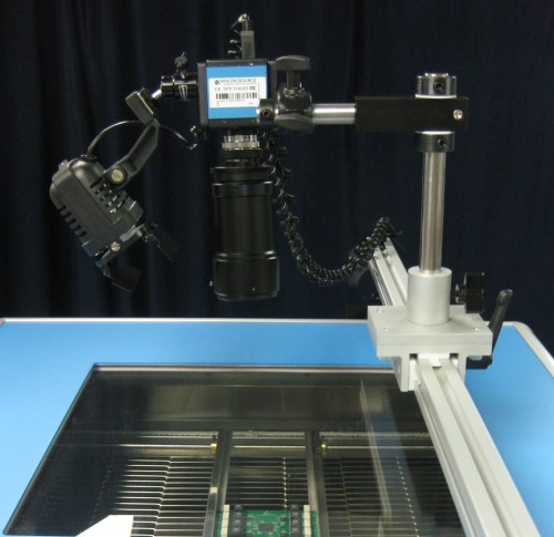
Upgraded video observation module for PRO 1600 Reflow Oven now allows taking still images and recording video during a reflow cycle. Camera may be focused and magnified at the solder paste joint level thereby providing visual feedback during the soldering process. Primary benefit of this feature is analysis and study of behavior of solder paste and SMT components during reflow soldering. It helps to identify, analyze, and ultimately to prevent defects.
The module includes a dual panel 16” X 16” high temperature rated glass cover, high resolution camera with optical and digital zoom, lighting system, multi-angle adjustable camera mounting, and an advanced Imaging Capture software.
Introduction
Components

Removal
After securing the motherboard by the board holder’s clamps, an operator installs a vacuum pick up tip and nozzle suitable for the BGA device. Implementing machine’s optics, the nozzle is aligned over the component. A pre-established profile is selected from the software’ library and Start icon is selected. At this point the process is hands-off. Rework station automatically drives the nozzle down to a board and covers the BGA. Machine then activates vacuum pick up tip so as to remove the component once reflow is achieved and the heating cycle is initiated. Figure 2 shows a nozzle covering the device during reflow.
Heating is precisely controlled by the software (Figure 3). It mimics an original profile with heat applied from both top and bottom sides of a board. Source of bottom heating is Quartz IR while the top side is forced air or nitrogen convection. As is shown in the video of removal, upon completion of reflow, the machine lifts a BGA off a board and moves nozzle up along Z axis to its starting point.


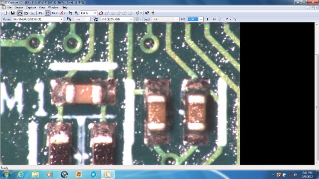
Residual solder remains on the board after removing a component. It takes the shape of Hershey’s kisses candy due to surface tension of molten solder. As a result of its uneven shape and volume, solder must be removed prior to installing a new component (Figure 4). This may be accomplished by using a vacuum de-soldering tool or more commonly by wicking solder with a copper braid and soldering iron.

Installation


Conclusion
In order to properly rework a BGA component, the rework station must contain features like split vision optics, software controlled sequencing and thermal management, and automation. These features not only simplify the process but also enable achieving high quality results on a consistent basis.